
Why Breaking Down the Monolithic Die?
Historically, the semiconductor industry relied on a monolithic die – a single silicon chip containing all functional units. This approach was cost-effective because the single-chip area remained manageable, and advanced packaging was both expensive and difficult to execute.
Today, two key factors make the single-chip approach inefficient:
- Slower Gains from Process Scaling: Moving to more advanced technology nodes yields smaller improvements in performance and power efficiency than before, while wafer manufacturing costs continue to rise
- Different Technology Node Requirements:
- Logic cores benefit directly from leading-edge nodes (e.g., 3nm/5nm)
- Analog and I/O circuits scale poorly on leading-edge nodes, which are expensive and difficult to manufacture without clear benefits
- Memories prioritize density rather than aggressive logic scaling. Using expensive logic processes for memory is wasteful
Breaking down the chip resolves this conflict: manufacture each functional block on its optimal process node to maximize individual yield, then package them together.
Architectural Trade-offs When Breaking Down Chips
Breaking a single chip into smaller pieces requires balancing several design choices:
| Design Driver | Considerations & Trade-offs |
| Interconnect Bandwidth | Functional blocks that exchange data frequently (like L3 Cache and Compute Cores) must sit close together. |
| Process Node Matching | Blocks with similar silicon manufacturing needs should stay on the same die. |
| Area vs. Yield Balance | Smaller dies have higher manufacturing yields per wafer, but using more dies increases package connections, assembly costs, and communication delays. Larger dies lower communication delays, but silicon yield drops quickly as die size grows. |
| Thermal Management | Placing high-power compute dies too close together traps heat locally, making cooling difficult. Spreading them out eases cooling, but increases the overall package size. |
| Design for Testability (DFT) | On a monolithic die, test points are easy to access inside the chip. In advanced packaging, many connection points are hidden between layers, making testing before and after assembly much harder. |
Packaging Architectures: 2D vs. 3D Definitions
According to Chapter 22 of the IEEE / SEMI / ASME Heterogeneous Integration Roadmap (HIR):
- 2D Architecture: An architecture where two or more active silicon devices are placed side-by-side on a package and are interconnected on the package
- 3D Architecture: An architecture where two or more active silicon devices are stacked and interconnected without using the package substrate
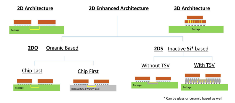
Each of the architectures has its own limitations:
- 2D Architecture is limited by package surface area. Adding more chips requires a larger base substrate, which makes the package more expensive and harder to build
- 3D Architecture is limited by thermal management and power delivery. Heat from the bottom chip must pass through the top chip to escape. Power must be delivered from the bottom chip all the way up to the top chip, increasing voltage drop over the longer electrical path
How 2D and 3D Architectures Are Built
TSMC’s CoWoS technology is a great case study for 2D architectures:
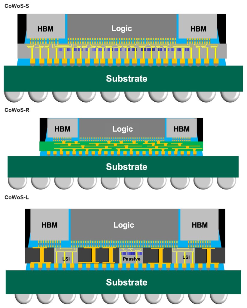
| Variant | Structure Material | Cost | Connection Density |
| CoWoS-S | Full Silicon Interposer with Through-Silicon Vias (TSVs) | Highest | Highest |
| CoWoS-R | Redistribution Layer (RDL) with Copper Wiring | Lowest | Lowest |
| CoWoS-L | Organic RDL Interposer with Local Silicon Interconnect (LSI) Bridges | Medium | Medium |
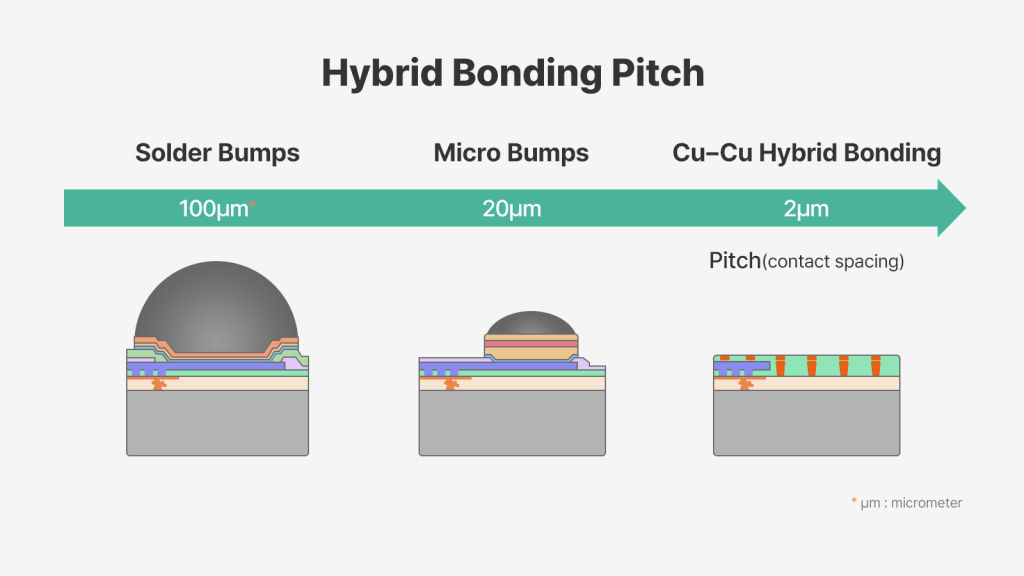
The following picture from SKHynix, shows some key 3D architecture differences:
TSMC’s SoIC technology is a great case study for 3D architectures:
- Traditional Microbumps (e.g., TSMC SoIC-P): Connects stacked dies using tiny solder bumps with underfill material in the gaps. Connection pitch sits between 25 and 40 microns. It is reliable, offers controlled yields, and has years of production history.
- Hybrid Bonding (e.g., TSMC SoIC-X): Removes solder bumps entirely. Copper pads and dielectric layers bond directly together face-to-face. Without solder taking up space, connection pitch drops below 10 microns.
Combining Both Technologies: AMD MI300 Series
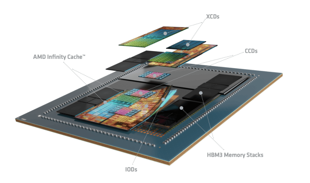
Modern AI chips often combine 2D and 3D packaging in a single system. For example, AMD MI300 Series AI Accelerators combine CPUs, GPUs, and memory into a massive unified package using TSMC’s advanced packaging ecosystem:
- Vertical Stacking (3D): 5nm compute dies (CPUs/GPUs) are stacked directly on top of 6nm Base I/O dies using TSMC SoIC direct hybrid bonding
- Horizontal Placement (2D): The stacked core modules sit side-by-side next to High Bandwidth Memory (HBM3) stacks on a CoWoS interposer
The Economic and Strategic Shift
For a long time, packaging was a simple, low-value step at the end of the chain: Its only job was to mount the chip safely on a board. Today, advanced packaging is a main bottleneck for delivering high-performance AI chips.
- High Packaging Costs: CoWoS packaging costs have grown from about $750 per chip (NVIDIA H100 generation) to $1,000–$1,100 (Blackwell B200 generation). A CoWoS interposer wafer now costs about the same as a full 7nm silicon wafer
- Capacity Bottlenecks: Advanced packaging capacity directly limits how many AI chips companies can ship. TSMC CoWoS lines remain fully booked, with major tech companies fighting to secure capacity
Advanced packaging is no longer just a manufacturing detail: It is now a key strategic decision alongside silicon technology node selection.
References:


Leave a Reply