The system board is mounted with fully-tested scannable ASIC SoCs, and scan-based ASIC testing is used to detect defects inside these SoCs. However, these internal scan chains are not useful to detect board-level faulty traces.

To detect faults on the system board, the concept of boundary scan and its associated industry standard JTAG (Joint Action Test Group) were introduced. Boundary scan ring is added to all JTAG-compliant chips on the board, and each chip’s ring is then daisy-chained to its neighbor’s ring. In addition, several JTAG pins are added to each chip, and to the board itself.
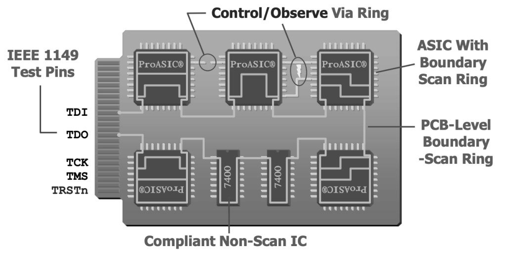
Boundary scan cells are inserted to chip I/O paths, between chip core and pads. These cells are more than just scannable flops, they are designed to be reversible, for either input or output paths.
To learn more, we recommend interviewees to study Chapter 10 of the book “VLSI Test Principles and Architectures: Design for Testability”. It is one of the most comprehensive guides to DFT methodology in the market.

References

Leave a comment