We briefly discussed the concept of scan-based ASIC testing, and there are certain rules associated with DFT, such that the SoC can achieve a good coverage.
We will cover a few DFT design guidelines in this post.
All Clocks Must Be Controllable by DFT Modes
This is done using a bypass mux in ATPG mode. For example, if certain flops are driven by an on-chip clock divider, insert a mux bypassing clock divider such that those flops are scannable.
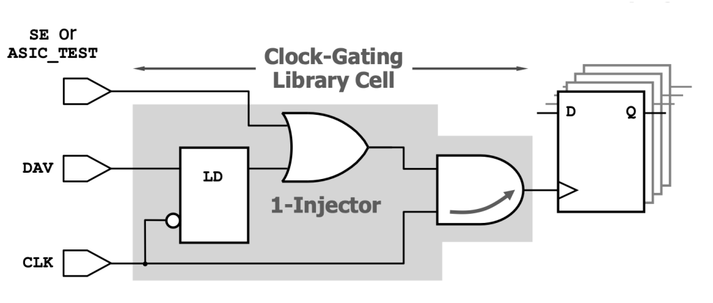
Separately, modern SoCs are using latch based clock gaters for power optimizations, and non-scan latches may result in hundreds of flops being excluded from any scan chain. One possible solution is to insert an OR gate into the clock gating cell, such that DFT clocks can reach the flops directly. Of course, power reduction is disabled while the chip is on ATE.
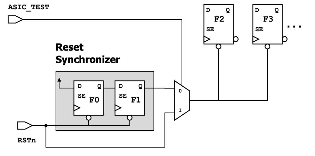
All Resets Must Be Controllable by DFT Modes
This is done using a bypass mux inside reset synchronizers in ATPG mode.
STA Must Close Timing for DFT Modes
STA must ensure timing closure for DFT modes, otherwise the chips will not work properly during testing.
It is common to see hold time violations in scan chains, as the scan chains are simple wires between scannable flops, and hold time violations do not depend on clock frequency.
Avoid Running Functional Patterns for Testing
Functional patterns are tedious and time-consuming to create, and they require more patterns to test a feature than the standard ATPG. DFT engineers should avoid running functional patterns for testing.
Proper Scan Chain Balancing & Planning
Testing is a cost overhead for SoCs. The faster we complete ATE, the lower the cost will be.
On one hand, one single long scan chain not only increases the ATE completion time, but also underutilizes ATE pattern memory space.
On the other hand, increasing the number of scan chains improves the test time, but results in more costs. For example, we may need more scan in and out pins at chip level, but chip level pins are a limited resource.
Therefore, proper scan chain balancing and planning are necessary during chip design phase.

Leave a comment