ATPG uses a method called internal scan, or scan-based ASIC testing to test sequential logic in the design. We will discuss scan-based ASIC testing in this post.
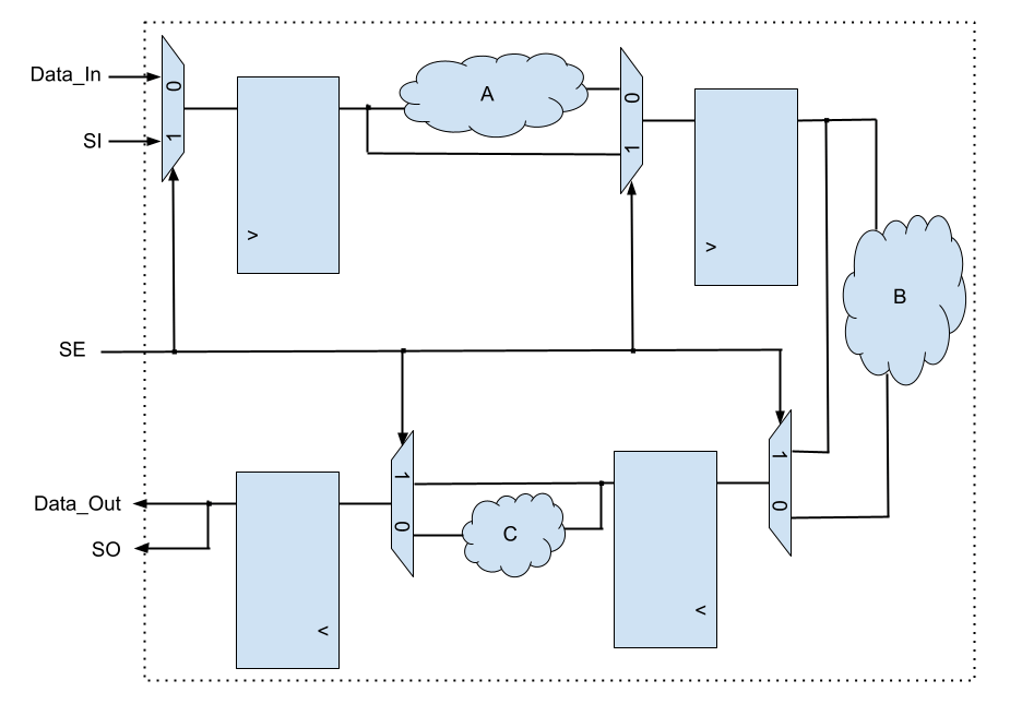
Internal scan methodology replaces the regular flops with scan flops. Compared to regular flops, scan flops have two extra inputs, SI (Scan Input) and SE (Scan Enable), and one extra output, SO (Scan Output). SI provides a dedicated input to load or pass a value to the scan flop directly. When SE is 1, SI supplies the input to the flop; When SE is 0, or normal functional mode, scan flop behaves like a regular flop. SO provides an extra output path for scan chains.

The scan insertion typically happens after logic synthesis, and the scan insertion toolkit will stitch these flops into scan chains. Scan chains enable chip level input propagation through the chain, and all the way to the chip level output. The diagram below shows a simple scan chain example.
During scan-based ASIC testing, there are 3 steps involved:
- Scan Shift-In: SE pin will be high, and scan data is shifted into the chain, one bit per clock cycle. It may take multiple cycles to fill a scan chain
- Scan Capture: SE pin will be low, and the scan flop outputs are applied to the inputs of the combinational logic between flop stages. The combinational logic outputs are captured in flops which these combinational logics are driving. Scan capture uses at-speed clock, such that the faults / defects are examined as if the chip is in functional mode
- Scan Shift-Out: SE pin will be high, and the scan flop outputs are shifted out from the scan chain to chip level outputs for further analysis, one bit per cycle. Scan shift-out can also take multiple clock cycles to complete
A special circuitry, called On-Chip Clock Controller (OCC), is used to provide the required clock sequence for internal scan. It is typically inserted per user clock domain. The waveform below shows the internal scan sequence with the use of OCC.

Note, for scan-based ASIC testing to work properly, there are certain rules and design guidelines that SoC engineers must follow. We will discuss them in the next post.
Internal scan is not only useful in scan-based ASIC testing, but also a powerful tool in post-silicon debugging, especially in debugging system hang conditions. We covered this in our book “Crack the Hardware Interview: Physical Design & Silicon Debug”.

To learn more, we recommend interviewees to study Chapter 2 of the book “VLSI Test Principles and Architectures: Design for Testability”. It is one of the most comprehensive guides to DFT methodology in the market.


Leave a comment